
Chip Design & Wafer Fabrication
Reliable, scaleable and cost-efficient acoustofluidic devices.
IDT & Chip Design
Functional acoustic wave and acoustofluidic devices are not created by simply drawing interdigital transducers (IDTs). Performance is often limited by subtle effects that are difficult to control without deep understanding of acoustic wave propagation, wave-structure interaction, fabrication constraints, and system requirements.
At SONOJET, we provide expert 2D-CAD layout services for Surface Acoustic Wave (SAW), Bulk Acoustic Wave (BAW), and other acoustic wave based chip devices, transforming simulation results and design specifications into fabrication-ready mask layouts.
Whether you look for a new transducer layout or improve existing ones, we have the expertise and resources to support you every step of the way.
Wafer Fabrication
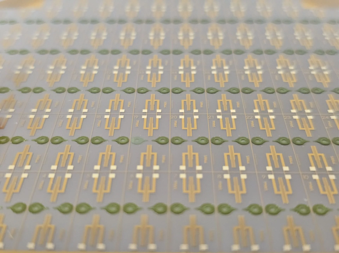
SONOJET offers wafer fabrication services dedicated to surface acoustic wave (SAW) based chip devices, providing a flexible platform for research, prototyping, and pilot production.
Our process flow is optimized for rapid prototyping by laser lithography, while maintaining the process control required for high-performance acoustic components.
Our production services include:
laser lithography (≥ 2.5 µm structure resolution)
metal evaporation (Al, Ti, Au, Pt, …)
passivation (high-quality SiO₂ sputtering)
reactive ion etching
up to 6 inch wafers (LiNbO₃, Si, Quartz, fused Silica)
epoxy lithography (dry-film photoresists) for wafer-scale integrated microfluidic channels and PDMS masters, using our patented technology
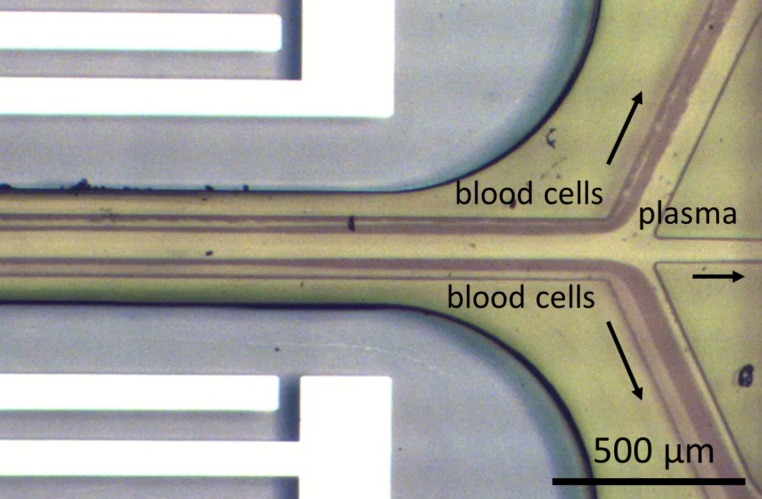
chip characterization (optical, electrical, structural, wave-field)
Integrated Microfluidics
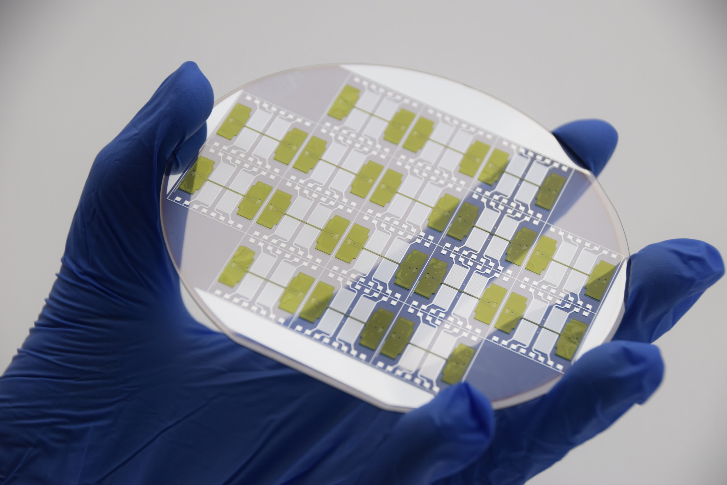
Advancing passive microfluidics with active functions opens up completely new possibilities for particle, cell, fluid and droplet handling. At SONOJET, we combine acoustic technology with integrated microfluidic structures to create next-generation lab-on-a-chip devices.
Take advantage of our patented expoxy-based dry film lithography technique to integrate SAW transducers and custom on-chip microchannel designs at full waferscale. Thus, we deliver highest possible geometry precision and reproducibilty for defined liquid control combined with mass-manufacturability of acoustofluidic chips.
We also provide prototyping and manufacturing of passive microchannels as well as conventional waferscale masters for your PDMS-based soft-lithography approach.
Chip Characterization
Functional acoustic wave devices and acoustofluidic devices are not created by simply drawing interdigital transducers (IDTs). Performance is often limited by subtle effects that are difficult to control without deep understanding of acoustic wave propagation, fabrication constraints, and system requirements.
At SONOJET, we provide expert 2D-CAD layout services for Surface Acoustic Wave and other acoustic wave based chip devices, transforming simulation results and design specifications into fabrication-ready mask layouts. Whether you are looking for a new transducer layout or improve existing ones, we have the expertise and resources to support you every step of the way.
From Prototyping to Series Production
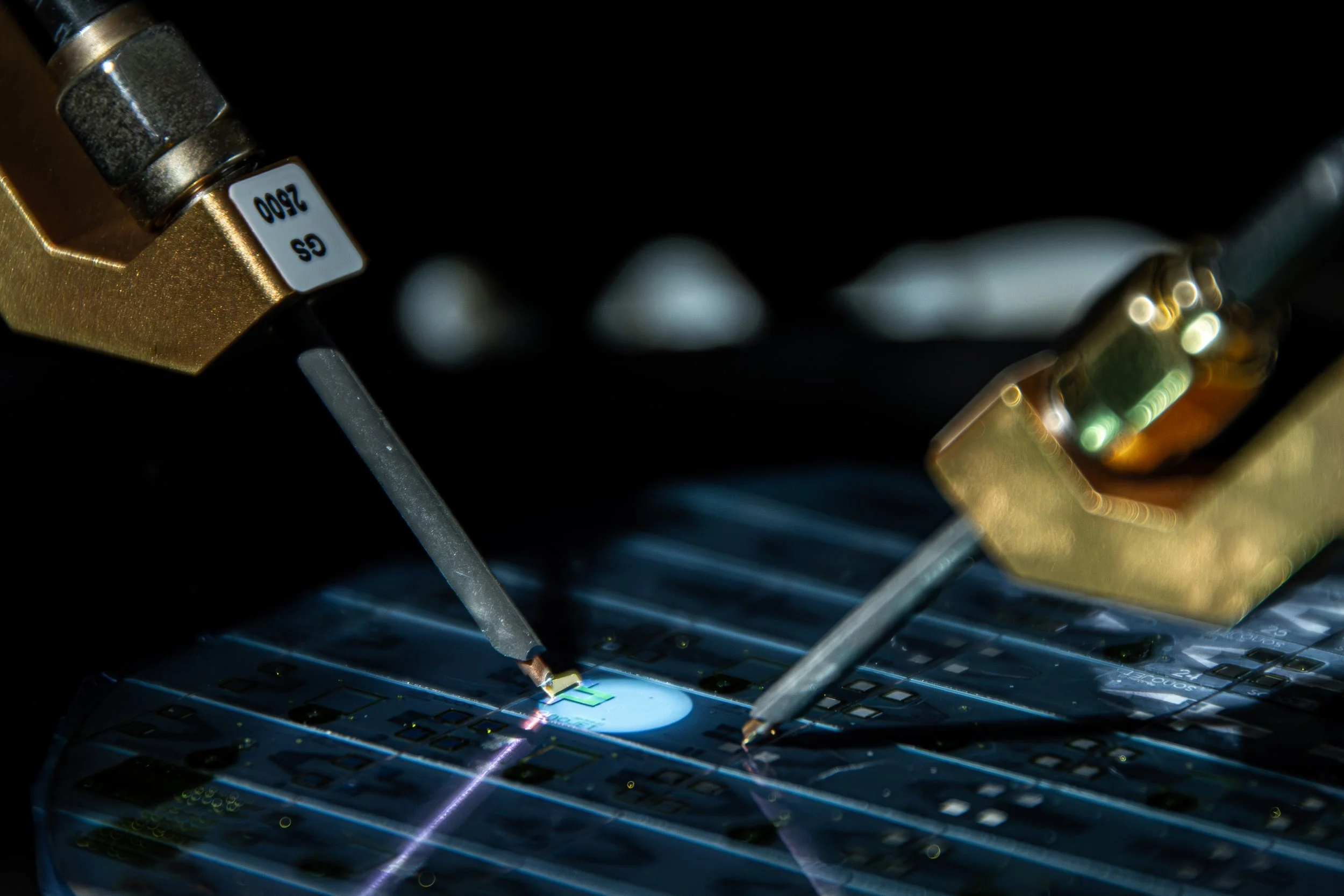
While SonoJet focuses on fast and cost-efficient prototype development and low-volume manufacturing, our partnership with SAW COMPONENTS Dresden GmbH enables a seamless transition from initial concepts to full-scale wafer fabrication and high-volume production. Together, we provide a complete manufacturing pathway — from device design and prototyping through industrial wafer processing, packaging, and scalable production.
Application Examples
acoustic manipulation of particles & cells
wafer-scale masters for PDMS soft-lithography approaches
acoustic mixing
of fluids & suspensions
acoustic jetting, aerosol & droplet generation